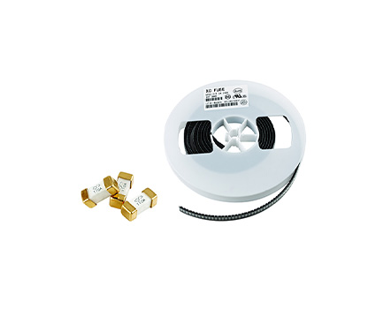
Most SMD fuses look like standard SMD devices, using single or multi-layer ceramic substrates. Some previous designs used epoxy glass fiber substrates similar to printed circuit boards. Its structure includes: a shell, a lower cover, quartz sand, a fuse, and two terminal blocks. The shell is a ceramic box like structure without a bottom surface, and the two terminal blocks are connected together through a suspended fuse set inside the shell, which is clamped on the edge of the shell. The basic fuse in the middle is a high conductivity material, such as copper, gold or copper tin, silver palladium alloy.
Depending on the type of substrate, the fuse can use laser fine tuned thick film deposits or chemically etched metal layers to achieve the desired performance parameters, and adhesive gold wires can also be used. Due to the determined shape and thickness, when subjected to overvoltage and the current reaches a certain level, the fuse will fuse within a certain period of time.
To achieve the function of this functional layer, the patch fuse must be protected from environmental conditions. In single-layer patch fuses, the surface of the fuse is usually coated with a layer of paint or epoxy resin. The substrate layer of the multi-layer patch fuse fuse itself has a protective effect. And they require low resistance SMD contacts.
Read recommendations: